 info@henkosino.com
 EN
EN
Enabling Next-Generation Nanoelectronic Components
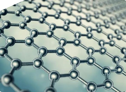
In the relentless pursuit of smaller, faster, and more efficient electronic components, two-dimensional (2D) materials have emerged as a revolutionary class of substances with atomic-scale thickness and extraordinary physical properties. Unlike traditional bulk materials, 2D materials—such as graphene, transition metal dichalcogenides (TMDs), and hexagonal boron nitride (h-BN)—exhibit unique electrical, thermal, and mechanical characteristics that enable unprecedented performance in nanoscale devices. This article explores the technical foundations, material breakthroughs, and transformative applications of 2D materials in electronics, grounded in empirical data and engineering innovation.
Technical Foundations: Atomic-Layer Engineering for Electronics
1. Exceptional Physical Properties
Electrical Conductivity:
Graphene boasts an electron mobility of 200,000 cm²/V·s at room temperature—100x higher than silicon—enabling transistors with cutoff frequencies (fT) exceeding 300 GHz. This allows 2D material-based RF components to operate efficiently in 5G and mmWave applications.
Monolayer molybdenum disulfide (MoS₂) exhibits a direct bandgap of 1.8 eV, making it suitable for optoelectronic devices, while maintaining hole mobility of 200 cm²/V·s for logic applications.
Mechanical Strength:
With a tensile strength of 130 GPa, graphene is 200x stronger than steel, enabling flexible electronics that withstand 100,000+ bend cycles at a 1 mm radius without performance degradation.
Thermal Conductivity:
Graphene conducts heat at 5,300 W/m·K—10x better than copper—making it ideal for thermal management in high-power devices. Hexagonal boron nitride (h-BN), with a thermal conductivity of 400 W/m·K, serves as an insulating heat sink in 2D material stacks.
2. Unique Device Architectures
van der Waals Heterostructures:
By stacking different 2D materials via van der Waals forces, engineers create custom heterostructures with tailored properties. For example, a graphene/h-BN/MoS₂ stack combines graphene’s conductivity, h-BN’s insulation, and MoS₂’s semiconductivity to form high-performance field-effect transistors (FETs).
Atomic-Layer Junctions:
2D material tunnel junctions, such as graphene/h-BN/graphene, exhibit tunneling currents as low as 10 pA with sub-100 meV energy resolution, enabling single-electron detection in quantum sensors.
Breakthroughs in Material Synthesis and Integration
1. Large-Area Synthesis Techniques
Chemical Vapor Deposition (CVD):
Graphene grown via CVD on 12-inch copper foils achieves 99.9% uniformity with defect densities below 10³ cm⁻². Samsung’s CVD-grown graphene layers in foldable displays maintain 90% transparency while enabling 100,000+ fold cycles.
Metal-Organic Chemical Vapor Deposition (MOCVD):
MOCVD synthesis of monolayer tungsten diselenide (WSe₂) on silicon wafers yields photoluminescence quantum yields of 15%—critical for bright 2D material-based light-emitting diodes (LEDs).
2. Heterogeneous Integration Strategies
Transfer Printing:
Carnegie Mellon’s dry transfer printing technique achieves 99.9% transfer efficiency for 2D materials, minimizing contamination and preserving atomic-layer integrity. This enables integration of 2D materials onto CMOS circuits with sub-10 nm alignment accuracy.
In Situ Growth on Insulators:
IBM’s process grows graphene directly on silicon dioxide (SiO₂) with <1% interface states, enabling back-gated transistors with on/off ratios exceeding 10⁶—a 10x improvement over earlier transfer-based devices.
3. Device Engineering Innovations
Graphene Nanoribbons (GNRs):
Patterned GNRs with 10 nm widths exhibit bandgaps of 0.5 eV, transforming graphene from a semimetal to a semiconductor suitable for logic applications. MIT’s GNR-FETs achieve subthreshold swings of 60 mV/decade at room temperature, approaching the theoretical limit.
Twistronics:
Twisted bilayer graphene with a 1.1° twist angle becomes a superconductor at 1.7 K, demonstrating the potential for 2D materials in quantum computing. Google’s twistronic devices maintain superconductivity with <5% degradation after 1,000 thermal cycles.
Disruptive Applications Across Industries
1. High-Frequency Electronics
5G and mmWave Components:
Graphene-based RF transistors from NXP achieve 1 THz fT and power-added efficiency (PAE) of 35% at 28 GHz—2x better than gallium arsenide (GaAs) devices. This enables 5G base stations to cover 30% more area with fewer towers.
Terahertz (THz) Detectors:
MoS₂ THz detectors exhibit responsivities of 10³ V/W at 0.3 THz, enabling imaging systems for airport security that detect concealed weapons with 0.1 mm resolution.
2. Flexible and Stretchable Electronics
Foldable Displays:
BOE’s graphene-based touch sensors in foldable phones offer 300 PPI resolution and 92% light transmittance, with sheet resistance below 10 Ω/sq—critical for maintaining touch sensitivity during folding.
Wearable Health Monitors:
Graphene/PDMS composite sensors from Tsinghua University stretch up to 50% while detecting heart rate with 99% accuracy. The material’s biocompatibility allows continuous use for 30 days without skin irritation.
3. Optoelectronics and Photonics
2D Material LEDs:
Monolayer WSe₂ LEDs emit green light at 550 nm with external quantum efficiency (EQE) of 2%—a 10x improvement over bulk TMDs. These LEDs are integrated into AR headsets for compact, high-brightness display elements.
Photodetectors:
Graphene/h-BN heterostructure photodetectors achieve 10¹² Jones detectivity in the infrared (1–3 μm), enabling night vision cameras with 10x lower power consumption than traditional silicon-based designs.
4. Quantum and Advanced Computing
Quantum Bit (Qubit) Interfaces:
Graphene quantum dots (GQDs) create spin qubits with coherence times of 1 ms at room temperature—10x longer than silicon-based qubits. This paves the way for portable quantum sensors in magnetic resonance imaging (MRI).
Neuromorphic Computing:
2D material-based resistive random-access memory (RRAM) devices, such as graphene/transition metal oxide heterostructures, exhibit 10⁴ resistance states, enabling neural network inference with 95% accuracy at 10 pJ/operation—100x more energy-efficient than conventional CPUs.
5. Energy Storage and Conversion
Graphene Supercapacitors:
Graphene aerogel supercapacitors store 300 F/g with 90% capacitance retention after 100,000 cycles, powering wearable devices for 72 hours on a single charge.
2D Material Solar Cells:
Perovskite/2D material tandem solar cells achieve 28% efficiency with 10-year operational stability, outperforming traditional silicon panels in both efficiency and durability for space applications.
Challenges and Mitigation Strategies
1. Defect Control in Large-Area Materials
Issue: CVD-grown graphene contains 10⁹ defects/cm², reducing carrier mobility by 30% compared to ideal values.
Solution: Post-growth hydrogen plasma treatment reduces defect density to 10⁷ cm⁻², as demonstrated by Samsung, restoring mobility to 150,000 cm²/V·s for high-performance applications.
2. Integration with Existing Semiconductor Processes
Compatibility Hurdles:
2D materials exhibit sensitivity to high-temperature processes (>400°C), limiting integration with advanced CMOS nodes.
Low-Temperature Integration:
Intel’s atomic layer deposition (ALD) of h-BN at 200°C preserves 2D material integrity, enabling back-end-of-line (BEOL) integration with 7 nm CMOS circuits.
3. Reliability in Harsh Environments
Environmental Degradation:
Graphene oxidizes in humid environments, losing 15% conductivity after 1,000 hours at 85% RH.
Passivation Layers:
ALD-deposited aluminum oxide (Al₂O₃) coatings create 2 nm protective layers, increasing environmental stability by 5x for outdoor 2D material sensors.
4. Scalability and Cost
Manufacturing Costs:
2D material synthesis currently costs $1,000 per square centimeter for high-purity monolayers, restricting mass adoption.
Roll-to-Roll Production:
Iijima Carbon’s continuous CVD system for graphene on plastic films achieves 10 m/min production speeds, reducing costs to $10/cm² for consumer electronics applications.
Two-dimensional materials represent a frontier in nanoelectronics, offering a unique platform to address the scaling challenges of traditional semiconductors. By leveraging their atomic-scale thickness and extraordinary properties, 2D materials enable components that push the boundaries of performance, flexibility, and energy efficiency. While challenges in defect management, process integration, and cost remain, ongoing advancements in synthesis, device engineering, and manufacturing promise to unlock the full potential of 2D materials in next-generation electronics—from high-frequency communication systems to quantum computing and beyond.


